AMD Next Horizon in San Francisco, California, Tuesday, November 6, 2018.
(Photography by Paul Sakuma Photography) www.PaulSakuma.com
— Launches World’s first 7nm High-performance GPU for Machine Learning and AI; Demonstrates World’s First High-performance 7nm x86 CPU Powered by “Zen 2” Processor Core and Breakthrough Chiplet Design —
— Amazon Web Services Announces Immediate Availability of AMD EPYC processor-powered Versions of Its Popular Instance Families —
Dubai, UAE — Nov. 7, 2018 — AMD (NASDAQ: AMD) demonstrated its total commitment to datacenter computing innovation at its Next Horizon event in San Francisco by detailing its upcoming 7nm compute and graphics product portfolio designed to extend the capabilities of the modern datacenter. During the event, AMD shared new specifics on its upcoming “Zen 2” processor core architecture, detailed its revolutionary chiplet-based x86 CPU design, launched the 7nm AMD Radeon Instinct™ MI60 graphics accelerator and provided the first public demonstration of its next-generation 7nm EPYC™ server processor codenamed “Rome”. Amazon Web Services (AWS), the world’s most comprehensive and broadly adopted cloud platform company, joined AMD at the event to announce the availability of three of its popular instance families on the Amazon Elastic Compute Cloud (EC2) powered by the AMD EPYC™ processor.
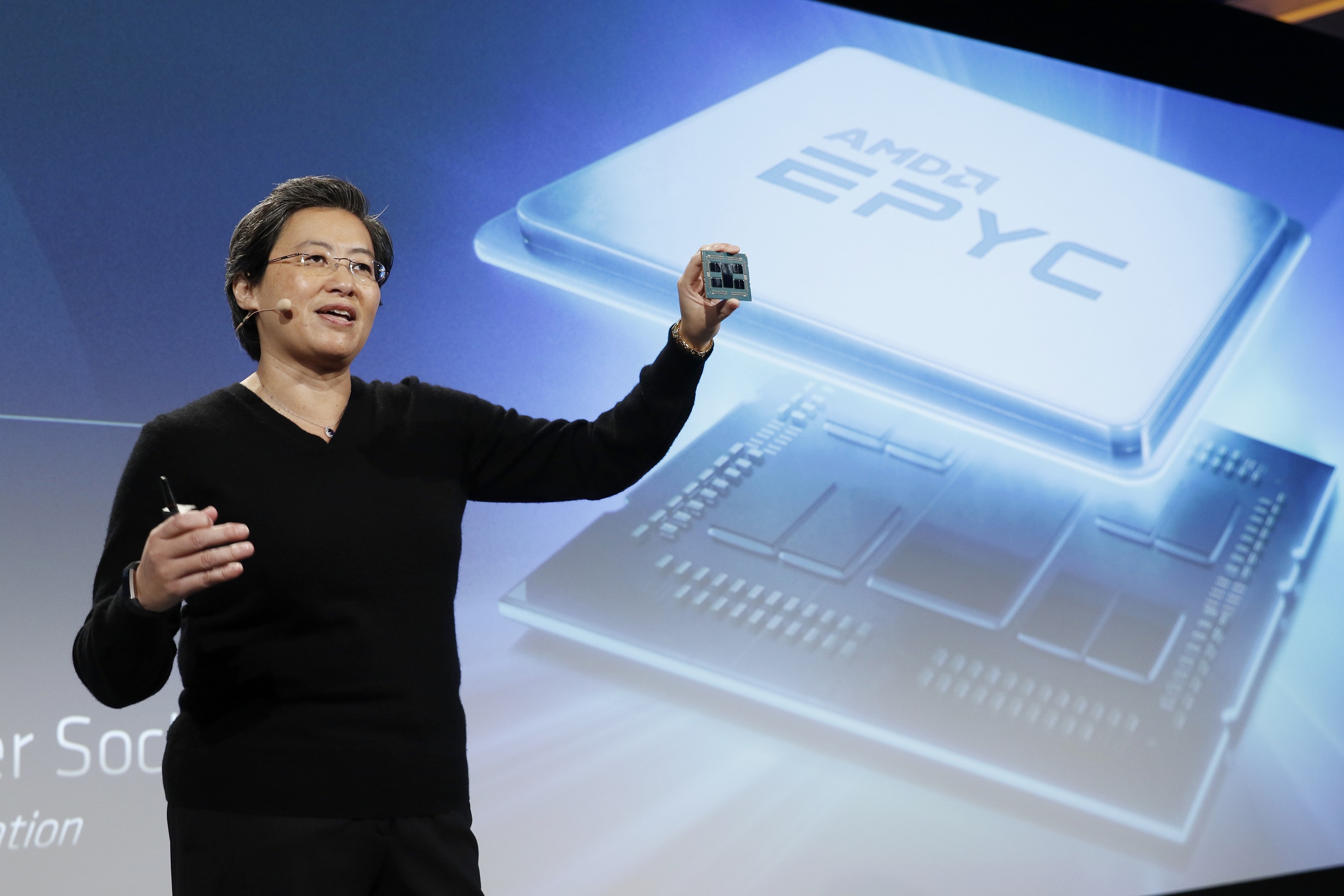
“The multi-year investments we have made in our datacenter hardware and software roadmaps are driving growing adoption of our CPUs and GPUs across cloud, enterprise and HPC customers,” said Dr. Lisa Su, president and CEO, AMD. “We are well positioned to accelerate our momentum as we introduce the industry’s broadest, most powerful portfolio of datacenter CPUs and GPUs featuring industry-leading 7nm process technology over the coming quarters.”
AMD Compute Architecture Updates
AMD for the first time detailed its upcoming “Zen 2” high-performance x86 CPU processor core that is the result of a revolutionary modular design methodology. This modular system design uses an enhanced version of AMD Infinity Fabric interconnect to link separate pieces of silicon (“chiplets”) within a single processor package. The multi-chip processor uses 7nm process technology for the “Zen 2” CPU cores that benefit from the advanced process technology, while leveraging a mature 14nm process technology for the input/output portion of the chip. The result is much higher performance – more CPU cores at the same power, and more cost-effective manufacture than traditional monolithic chip designs.
Combining this breakthrough design methodology with the benefits of TSMC’s leading-edge 7nm process technology, “Zen 2” delivers significant performance, power consumption and density generational improvements that can help reduce datacenter operating costs, carbon footprint and cooling requirements. Other key generational advances over the award-winning “Zen” core include:
- An improved execution pipeline, feeding its compute engines more efficiently.
- Front-end advances – improved branch predictor, better instruction pre-fetching, re-optimized instruction cache and larger op cache.
- Floating point enhancements – doubled floating point width to 256-bit and load/store bandwidth, increased dispatch/retire bandwidth and maintained high throughput for all modes.
- Advanced security features – Hardware-enhanced Spectre mitigations, taking software migration and hardening it into the design, and increased flexibility of memory encryption.
Multiple 7nm-based AMD products are now in development, including next-generation AMD EPYC CPUs and AMD Radeon Instinct GPUs, both of which AMD detailed and demonstrated at the event. Additionally, the company shared that its follow-on 7nm+-based “Zen 3” and “Zen 4” x86 core architectures are on-track.
AMD EPYC Server CPU Updates
Reinforcing the growing momentum achieved with its current-generation AMD EPYC processors, Matt Garman, vice president of compute services at AWS joined AMD on-stage at the event to announce the immediate availability of the first AMD EPYC processor-based instances on Amazon Elastic Compute Cloud (EC2). Part of AWS’s popular instance families, the new AMD EPYC processor-powered offerings feature industry-leading core density and memory bandwidth. This results in exceptional performance-per-dollar for general purpose and memory-optimized workloads, driven by the core density of AMD EPYC processors that offer M5a and T3a customers a balance of compute, memory, and networking resources for web and application servers, backend servers for enterprise applications, and test/development environments with seamless application migration. For R5a customers, the memory bandwidth advantage of AMD EPYC processors is ideal for in-memory processing, data mining, and dynamic data processing.
AMD also disclosed new details and delivered performance previews of its next-generation EPYC processors codenamed “Rome”:
- Processor enhancements including up to 64 “Zen 2” cores, increased instructions-per-cycle[i] and leadership compute, I/O and memory bandwidth[ii].
- Platform enhancements including the industry’s first PCIe 4.0-capable x86 server processor with double the bandwidth per channel[iii] to dramatically improve datacenter accelerator performance.
- Double the compute performance per socket[iv] and four times the floating point performance per socket[v] compared to current AMD EPYC processors.
- Socket compatibility with today’s AMD EPYC server platforms.
AMD demonstrated the performance and platform advantages of its next-generation EPYC processor with two demos during the event:
- A pre-production single-socket next-generation AMD EPYC processor outperforming a commercially available top-of-the-line Intel dual processor Xeon server running the computationally-intensive, industry standard “C-Ray” benchmark[vi].
- The industry’s first x86 PCIe 4.0-capable platform demo, featuring a Radeon Instinct MI60 processor to accelerate image recognition.
“Rome” is sampling with customers now and is expected to be the world’s first high-performance x86 7nm CPU.
AMD Datacenter Graphics Updates
AMD launched the world’s first 7nm GPUs and the industry’s only hardware-virtualized GPUs – the AMD Radeon Instinct MI60 and MI50 – which are scheduled to ship to customers this quarter. These new graphics cards are based on the high-performance, flexible “Vega” architecture and are specifically designed for machine learning and artificial intelligence (AI), delivering higher levels of floating-point performance[vii], greater efficiencies[viii] and new features for datacenter deployments. A live demonstration during the event showed the flagship AMD Radeon Instinct MI60 running real-time training, inference and image classification.
In addition to new hardware announcements AMD also announced ROCm 2.0, a new version of its open software platform for accelerated computing that includes new math libraries, broader software framework support, and optimized deep learning operations. ROCm 2.0 has also been upstreamed for Linux kernel distributions, extending ROCm access to millions of Linux developers and users. Designed for scale, ROCm allows customers to deploy high-performance, energy-efficient heterogeneous computing systems in an open environment.
Presentations from the event are available now on at www.amd.com/NextHorizon. A full replay will be available within 12 hours and will remain available for approximately one year.
Supporting Resources
- Visit the Next Horizon event webpage for event materials
- Become a fan of AMD on Facebook
- Follow AMD on Twitter
About AMD
For more than 45 years AMD has driven innovation in high-performance computing, graphics and visualization technologies ― the building blocks for gaming, immersive platforms and the datacenter. Hundreds of millions of consumers, leading Fortune 500 businesses and cutting-edge scientific research facilities around the world rely on AMD technology daily to improve how they live, work and play. AMD employees around the world are focused on building great products that push the boundaries of what is possible. For more information about how AMD is enabling today and inspiring tomorrow, visit the AMD (NASDAQ: AMD) website, blog, Facebook and Twitter pages.
Cautionary Statement
This press release contains forward-looking statements concerning Advanced Micro Devices, Inc. (AMD) including the features, functionality, availability, timing, deployment and expectations of AMD future products and technologies, including “Zen 2,” “Zen 3,” “Zen 4,” “Rome,” AMD Radeon Instinct™ MI60 and MI50 accelerators and the ROCm 2.0 open software platform; AMD driving growing adoption in its CPUs and GPUs across cloud, enterprise and HPC customers; AMD being well positioned to accelerate its momentum through the introduction of AMD’s datacenter portfolio in the coming quarters; and expected benefits from EPYC™ based AWS R5, M5 and T3 instances, which are made pursuant to the Safe Harbor provisions of the Private Securities Litigation Reform Act of 1995. Forward-looking statements are commonly identified by words such as “would,” “intends,” “believes,” “expects,” “may,” “will,” “should,” “seeks,” “intends,” “plans,” “pro forma,” “estimates,” “anticipates,” or the negative of these words and phrases, other variations of these words and phrases or comparable terminology. Investors are cautioned that the forward-looking statements in this document are based on current beliefs, assumptions and expectations, speak only as of the date of this document and involve risks and uncertainties that could cause actual results to differ materially from current expectations. Such statements are subject to certain known and unknown risks and uncertainties, many of which are difficult to predict and generally beyond AMD’s control, that could cause actual results and other future events to differ materially from those expressed in, or implied or projected by, the forward-looking information and statements. Material factors that could cause actual results to differ materially from current expectations include, without limitation, the following: Intel Corporation’s dominance of the microprocessor market and its aggressive business practices may limit AMD’s ability to compete effectively; AMD has a wafer supply agreement with GF with obligations to purchase all of its microprocessor and APU product requirements, and a certain portion of its GPU product requirements, from GLOBALFOUNDRIES Inc. (GF) with limited exceptions. If GF is not able to satisfy AMD’s manufacturing requirements, its business could be adversely impacted; AMD relies on third parties to manufacture its products, and if they are unable to do so on a timely basis in sufficient quantities and using competitive technologies, AMD’s business could be materially adversely affected; failure to achieve expected manufacturing yields for AMD’s products could negatively impact its financial results; the success of AMD’s business is dependent upon its ability to introduce products on a timely basis with features and performance levels that provide value to its customers while supporting and coinciding with significant industry transitions; if AMD cannot generate sufficient revenue and operating cash flow or obtain external financing, it may face a cash shortfall and be unable to make all of its planned investments in research and development or other strategic investments; the loss of a significant customer may have a material adverse effect on AMD; AMD’s receipt of revenue from its semi-custom SoC products is dependent upon its technology being designed into third-party products and the success of those products; AMD products may be subject to security vulnerabilities that could have a material adverse effect on AMD; data breaches and cyber-attacks could compromise AMD’s intellectual property or other sensitive information, be costly to remediate and cause significant damage to its business and reputation; AMD’s operating results are subject to quarterly and seasonal sales patterns; global economic uncertainty may adversely impact AMD’s business and operating results; AMD may not be able to generate sufficient cash to service its debt obligations or meet its working capital requirements; AMD has a large amount of indebtedness which could adversely affect its financial position and prevent it from implementing its strategy or fulfilling its contractual obligations; the agreements governing AMD’s notes and the Secured Revolving Line of Credit impose restrictions on AMD that may adversely affect its ability to operate its business; the markets in which AMD’s products are sold are highly competitive; AMD’s issuance to West Coast Hitech L.P. (WCH) of warrants to purchase 75 million shares of its common stock, if and when exercised, will dilute the ownership interests of its existing stockholders, and the conversion of the 2.125% Convertible Senior Notes due 2026 may dilute the ownership interest of its existing stockholders, or may otherwise depress the price of its common stock; uncertainties involving the ordering and shipment of AMD’s products could materially adversely affect it; the demand for AMD’s products depends in part on the market conditions in the industries into which they are sold. Fluctuations in demand for AMD’s products or a market decline in any of these industries could have a material adverse effect on its results of operations; AMD’s ability to design and introduce new products in a timely manner is dependent upon third-party intellectual property; AMD depends on third-party companies for the design, manufacture and supply of motherboards, software and other computer platform components to support its business; if AMD loses Microsoft Corporation’s support for its products or other software vendors do not design and develop software to run on AMD’s products, its ability to sell its products could be materially adversely affected; and AMD’s reliance on third-party distributors and AIB partners subjects it to certain risks. Investors are urged to review in detail the risks and uncertainties in AMD’s Securities and Exchange Commission filings,
AMD, the AMD Arrow logo, EPYC, Radeon and combinations thereof, are trademarks of Advanced Micro Devices, Inc. Other names are for informational purposes only and may be trademarks of their respective owners.
[i] Estimated increase in instructions per cycle (IPC) is based on AMD internal testing for “Zen 2” across microbenchmarks, measured at 4.53 IPC for DKERN +RSA compared to prior “Zen 1” generation CPU (measured at 3.5 IPC for DKERN + RSA) using combined floating point and integer benchmarks.
[ii] NAP-42 – AMD EPYC™ 7601 processor supports up to 8 channels of DDR4-2667, versus the Xeon Platinum 8180 processor at 6 channels of DDR4-2667. NAP-43 – AMD EPYC 7601 processor includes up to 32 CPU cores versus the Xeon Platinum 8180 processor with 28 CPU cores.
NAP-44 – A single AMD EPYC™ 7601 processor offers up to 2TB/processor (x 2 = 4TB), versus a single Xeon Platinum 8180 processor at 768Gb/processor (x 2 = 1.54TB). NAP-56 – AMD EPYC™ processor supports up to 128 PCIe® Gen 3 I/O lanes (in both 1 and 2-socket configuration), versus the Intel® Xeon® SP Series processor supporting a maximum of 48 lanes PCIe® Gen 3 per CPU, plus 20 lanes in the chipset (max of 68 lanes on 1 socket and 116 lanes on 2 socket).
Based on “Zen 2” design parameters versus “Zen1” and currently shipping products – core count increase from 32 to up to 64 per socket. Memory bandwidth with up to 3200Gb/s memory speed across eight memory channels, I/O leadership extending to PCIeGen4.
[iii] Per Silicon Labs, provider of the PCIe Gen 4 solutions. (website here: https://www.silabs.com/community/blog.entry.html/2015/12/04/what_is_pcie_gen4a-oobp). PCIe Gen4 is a new standardized data transfer bus that will double the data transfer rate per lane of the prior Gen3 revision from 8.0 GT/s (gigatransfers/second) to 16.0 GT/s. This means that a single PCIe Gen4 interconnection will allow data rate transfers of up to 2GB/s (gigabytes/second), and a full 16 slot PCIe Gen4 interconnection for graphics cards and high-end solid state drives will allow data transfer rates of up to 32GB/s.
[iv] Testing performed by AMD Engineering as of October 2018 using AMD reference system with a pre-production “Rome” engineering sample, where “Rome” scored approximately 2x higher compared to “Naples” System.
[v] Estimated generational increase based upon AMD internal design specifications for “Zen 2” compared to “Zen 1”. “Zen 2” has 2X the core density of “Zen 1”, and when multiplied by 2X peak FLOPs per core, at the same frequency, results in 4X the FLOPs in throughput.
[vi] Estimates based on AMD internal testing as of November 6, 2018 in AMD “Ethanol” reference system (Oct 2018?) AMD EPYC™-based system configuration with AMD “Rome” Development Chassis with an EthanolX development board featuring a single next generation AMD EPYC (“Rome”) processor with a total of XXXXX DIMMs at XXXXX; versus Intel -based system configured with Supermicro’s SYS-1029U-TRTP; OS: Ubuntu 7.3.0-27ubuntu1~18.04; Linux: 4.15.0-36-generic; Compiler: GCC 7.3.0 with 2x Intel(R) Xeon(R) Platinum 8180M CPU, 24x32GB at 2666 MHz. The AMD “Rome” 1P server completes the C-Ray demo in ~ XXXXX sec and the Intel 8180M completes the benchmark in ~ XXXXX sec. Benchmark testing data redacted by AMD for confidentiality purposes, full disclosure will be available after launch.
[vii] As of Oct 22, 2018. The results calculated on for Radeon Instinct MI60 designed with Vega 7nm FinFET process technology resulted in 29.5 TFLOPS half precision (FP16), 14.8 TFLOPS single precision (FP32) and 7.4 TFLOPS double precision (FP64) peak theoretical floating-point performance. This performance increase is achieved with an improved transistor count of 13.2 billion on a smaller die size of 331.46mm2 then previous Gen MI25 GPU products with the same 300W power envelope.
The results calculated for Radeon Instinct MI50 designed with Vega 7nm FinFET process technology resulted in 26.8 TFLOPS peak half precision (FP16), 13.4 TFLOPS peak single precision (FP32) and 6.7 TFLOPS peak double precision (FP64) floating-point performance. This performance increase is achieved with an improved transistor count of 13.2 billion on a smaller die size of 331.46mm2 than previous Gen MI25 GPU products with the same 300W power envelope.
The results calculated for Radeon Instinct MI25 GPU based on the “Vega10” architecture resulted in 24.6 TFLOPS peak half precision (FP16), 12.3 TFLOPS peak single precision (FP32) and 768 GFLOPS peak double precision (FP64) floating-point performance. This performance is achieved with a transistor count of 12.5 billion on a die size of 494.8mm2 with 300W power envelope.
AMD TFLOPS calculations conducted with the following equation for Radeon Instinct MI25, MI50, and MI60 GPUs: FLOPS calculations are performed by taking the engine clock from the highest DPM state and multiplying it by xx CUs per GPU. Then, multiplying that number by xx stream processors, which exist in each CU. Then, that number is multiplied by 2 FLOPS per clock for FP32 and 4 FLOPS per clock for FP16. To calculate FP64 TFLOPS rate for Vega 7nm products MI50 and MI60 a 1/2 rate is used and for “Vega10” architecture based MI25 a 1/16th rate is used.
TFLOP calculations for MI50 and MI60 GPUs can be found at https://www.amd.com/en/products/professional-graphics/instinct-mi50 and https://www.amd.com/en/products/professional-graphics/instinct-mi60
| GFLOPS per Watt | |||
| MI25 | MI50 | MI60 | |
| FP16 | 0.082 | 0.089 | 0.098 |
| FP32 | 0.041 | 0.045 | 0.049 |
| FP64 | 0.003 | 0.022 | 0.025 |
Industry supporting documents / web pages:
http://www.tsmc.com/english/dedicatedFoundry/technology/7nm.htm
AMD has not independently tested or verified external/third party results/data and bears no responsibility for any errors or omissions therein.
RIV-2
[viii] Radeon Instinct™ MI60 contains 13.2 billion transistors on a package size of 331.46mm2, while the previous generation Radeon Instinct™ MI25 had 12.5 billion transistors on a package size of 494.8mm2 – a 58% improvement in number of transistors per mm2.